Semiconductors
Related: EE 331 - Devices and Circuit
Notes
Semiconductor: A semi conductor is a material that has a conductivity somewhere between an insulator and a conductor.
When you have a semiconductor material, like pure silicone, you have an assortment of silicon atoms that each have 8 valence electrons
If external energy is applied (usually in the form of light or heat) these electrons can break free from their atoms.
Since energy is required for an electron to go from bonded to free, the energy of free electrons should be more than that of bonded electrons.
The wider the band gap, the more energy required to bridge that gap.
Video Series Start
Semiconductors have two current carriers - electrons and holes
Free electrons are produced when thermal energy rises enough to cause valence electrons to jump to the conduction band. The number of holes left is equal to the number of free electrons that crossed the gap.
To improve conductivity, intrinsic(pure) semi conductors can be doped.
Semiconductors Doped with phosphorous(or other 5 valence electron atoms) have more free electrons and are known as n-type since the majority of the current carriers are electrons.
Semiconductors doped with Boron (or other 3 valence electron atoms), the number of holes are increased, and are known as p-type conductors since the majority of the current carriers are holes.
Doping a semiconductor changes it from intrinsic to extrinsic.
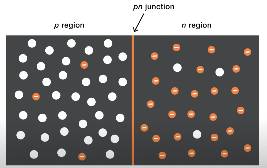
Combining N and P type materials creates an area known as the P-N Junction
Band Gap
The difference in energy between the band gap and conduction gap is known as the band gap.
The larger the gap, the harder it is for valence electrons to make the jump
Covalent Bonds form when electrons are shared between atoms.
When Free Electrons break free from their bond. This leaves "holes" in the material structure
Insulators have the largest band gap
Conductors have the smallest band gap (none)...the valence and conduction gaps overlap
Covalent Bonds form when electrons are shared between atoms.
When Free Electrons break free from their bond. This leaves "holes" in the material structure
When you put a voltage source across an intrinsic silicone material the free electrons will be attracted to the positive end of the voltage source (negative attracted to positive). This is known as Electron Current. This happens in the conduction band
Hole Current occurs in the valence band occurs when electrons shift to fill holes left by leaving free electrons.
Diodes
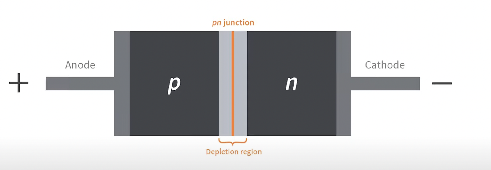
One way valve for electricity (P.A.N.I.C) Positive Anode, Negative is Cathode
PN Junction

P Region, the majority carriers are holes,
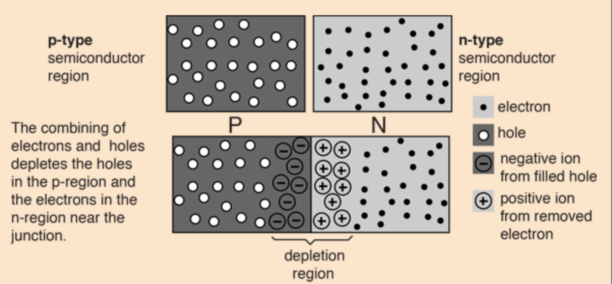
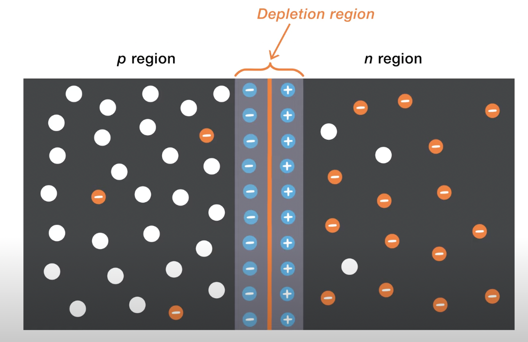
The depletion region is the area around the P-N Junction where electrons have diffused across the region and creates a layer of positive and negative charges. This is named such because the charge carriers are depleted. This region is formed almost instantly and is very small in relation to the p and n regions.


This creates a field that prevents electrons from the n region from flowing across to the p region
Forward Bias
When a voltage source is connected in forward bias with a Diode, the negative side pushes the majority carriers in the N region towards the PN junction. This is Electron Current. This allows them to overcome the barrier of the PN Junction and move into the P region. This allows electrons to fill the holes in the P region. In other-words, the holes provide a pathway. This causes the depletion region to narrow.
Reverse Bias
When you connect a voltage source to a diode in reverse bias (negative to P region, positive to N region). You draw free electrons out of the N region and holes out of the P region. This widens the Depletion region as it leaves a charge behind on each side
For Si atoms, the band gap
For Ge atoms, the band gap
1 electron volt is
Current Density(
However, usually since
When a charge is applied, free electrons tend to move to a positive charge. The "holes" they leave behind tend to propagate to the negative charge when this happens, we have a process known as Mobility.
Mobility =
is the magnitude of electron drift velocity caused by the electric field is the magnitude of the electric field applied to the material is the electron mobility
When you have electron mobility, you should have the same number of "holes" as free electrons, this is known as EHP or Electron Hole Pair.
Hole mobility is slower than electron mobility due to the fact that free electrons can move more easily
Intrinsic Semiconductors
Intrinsic Semiconductors are semiconductors in their ideal, purest elemental state.
Since
When talking about
For silicon,
Doped Semiconductors
To change the conductive properties of a semiconductor, we can "dope" them.
Doping means intentionally introducing impurities into an intrinsic semiconductors in order to modify its properties. These are also known as extrinsic semiconductors.
In general, there are two types of doped semiconductors
mobility depends on material
N-Type
N-Type semiconductors have electrons with a negative charge. In general, there are more electrons than "holes".